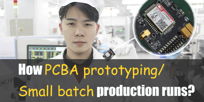
How PCBA Prototyping& Small Batch Production Run
Making 1pcs of PCBA prototyping board for debugging is really not easy for hardware engineers/ makers, how PCBA prototyping and small batch production run in a PCBA fab?

There are huge amounts of makers and hardware startups begun the creation of new hardware products, a simple but challenging work for them is the PCBA prototyping and small batch production. That is, making 1pcs of PCBA prototyping board for debugging is really not easy for hardware engineers/ makers, there are so many works to do for that include the PCB/ components/ soldering/ programming/ testing, etc. After the prototyping board passed, it is also not easy for the product manager to set a 100 pcs production, to have a try if the community would be interest in the product. Traditional factories will not be interested in producing a product with 100 pcs, they want 100K~; The product manager will need to try to persuade the factory: hey, this product has good furthers, that you will get big orders as the small batch production confirmed.
Thanks to Shenzhen, Asia's largest electronic market and plenty of electronic companies. Now, customers can get a much easier way to prototype their ideas, and produce them with any quantity that they would love to. With this “Smart Prototyping& Small Batch Production”, the designers can get their design into a real board in a short lead time and acceptable price, or manufacture 100 pcs to have a try if they work in the market, with a small investment.
A Standard PCBA Prototyping & Small Batch Production Runs as follows:
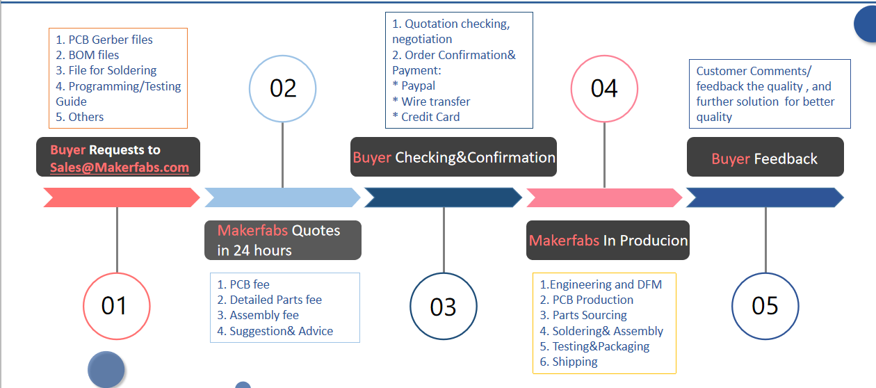
1. Designer Requests
Designers find one “Smart PCBA Prototyping & Small Batch Production” vendor in Shenzhen, for example, Makerfabs (check our turnkey PCBA service page), and send a request to the PCBA fab, in which explanation of what boards want, what’s the quantity, and the related production files:
1.1.) PCB Gerber Files And The Specs
This file is for PCB production, using the RS-274x format as it is the most widely used PCB file in Shenzhen. Remember that the Drill file(PCB name.txt ) also needed. PCB specs, include the color/ pads finish/ thickness/ copper weight. The most popular color is green, while some other colors such as blue/ red/ white/ yellow/ black also available, but maybe some extra fee for those un-popular colors. The pads finish can be Hasl/ ENIG, or some others, based on customers' requests.
1.2.) BOM List(Bill of Materials)
This is the most important file and often the mistakes happen here.
Some Tips:
-
List the same components/ items in the same row;
-
Mouser/ Digikey parts number would help to avoid misunderstanding.
1.3.) Parting Mapping File For Soldering
This is not mandatory. Distinct silkscreen on the PCB boards would also work for hand soldering. If there is no, or not enough silkscreens, a mapping file is needed.
2. Vendor Quotes
As receiving the customers' PCB assembly request, the vendor will estimate the total PCBA manufacturing cost. For a prototype PCBA production, the main cost includes:
2.1.) PCB Fee
Based on the PCB specs and production difficulty. Normally, the PCBA vendors will not produce the PCB by themselves, the PCB will be produced by the PCB factory. There are some “Express PCB” factories in Shenzhen, such as the HQ PCB and JLC PCB, that can provide the PCB with low starting fee(Less than 10$)and short lead time, but the quantity relative low, just fit for those prototyping productions and lower spec requirements. If the customer needs the PCB quality higher, or the PCB spec is high, for example, 6 layer PCB, the minimum trace interface 4 mils, some industry-level PCB factory may be needed. The starting fee would be higher, and the lead time is longer, normally 7~10 days.
2.2.) BOM List Fee
It is indeed there are some PCBA vendors can auto analysis the BOM list, if the customer provides a standard BOM list with Mouser/ Digikey code or vendor internal codes for all the components, but the disadvantage is obvious: it needs the customer provides all the parts numbers, but it is time-cost for the customer to do this when simple components needed such as a 1uf 0603 resistor, and also the price will be high, as the system will fetch price from Mouser/ Digikey directly. Actually in Shenzhen, for some components, a much lower price than Digikey/ Mouser is available. A more ensured, but the low-efficiency way is reviewing the BOM list by human. For some IC, the Shenzhen price would be much lower than that of Mouser/ Digikey, that a more completive price can be given to the circuit board designer.
2.3.) Soldering&Assembly Fee
Soldering and some other works such as programming and testing. In Shenzhen, there are plenty of soldering factories dedicated to this, but the starting fee is high for prototyping and small batch assembly, as actually there are a lot of works to start a PCBA production. The special PCBA prototyping &small batch production vendors organize all the small productions together and make this kind of production “Smart” with lower cost and shorter lead time.
2.4.) Shipping Fee
In Shenzhen, the DHL/ FedEx/ UPS are available with completive price. Besides, as Shenzhen not far from Hong Kong, some companies use the shipping service in Hong Kong, with even lower shipping costs.
3. Negotiating and Customer Paying
After negotiating, the designer pays the money. It is safer to use PayPal for the buyers, as PayPal would be a good 3-rd party to ensure the money is safe. The disadvantage of PayPal is the charge fee, charges about 3.5%~4%, so for the larger transactions and trusty parter, some other payment methodis also popular used, such as the wire transfer.
4. Production Start
It is really not a simple work to explain this process, very rough steps:
4.1.) Engineering
Need to firstly check how the PCB production and paneling, and how the boards will be soldered, and if there are any special requests, how the boards testing... That is, a detailed production guide is needed to control the whole production.
4.2.) Start the PCB Production
Normally 3~5 days for prototyping and 5~8 days for small batch production, based on the PCB specs and quantity.
4.3.) Preparing the Components
This is the most important step in the whole production for the PCBA prototyping and small batch assembly, that absolutely unlike the traditional mass production. In PCBA mass production, all the components are stable, the related sourcing man can check again and again the price, the certifications, slowly. But in the prototyping &small batch production, this must be done quickly, it needs really experienced components engineers, and stable& reliable vendors, to provide these components with low volume and completive price, and of course the most important, ensured the quality. This is not a work for one day, need a long time to find & cooperate the most proper vendors.
4.4.) Soldering& Assembly
The vendor may solder all the PCB themselves or find some other “bare soldering factory” to help, with human soldering or pick-n-place machine. This is really a long story, that we will discuss in a separate article later.
4.5.) Washing and Visual Checking
Wash the boards to keep them good looking, and check if there is anything wrong. This step needs experienced QC workers to do it. If there is a functional checking request, do them here.
4.6.) Repairing
It is almost impossible to ensure a 100% pass rate in production. If 100 pcs were produced, it is a good production if 95 pcs passed. An experienced soldering man needed here to repair the failed boards.
4.7.) Packaging
For international shipping, it is important to package all the boards safely. Remember the package will be thrown back and force by the DHL workers, it is better to ensure all the boards in safe with good protection in the package.
5. Ship the Package to Customer
Shipping the PCBAs to customers, And track the shipment until the package arrived at the buyer. This is not the end, get the feedback of the buyer. If any mistake happened, analyze the reason, and take the related responsibility!
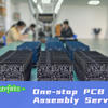
Check our video to learn how to assembly the PCB in Makerfabs factory:
@Dear makers,
Pls feel free to contact Makerfabs at service@makerfabs.com if you are finding an agile and reliable PCB Assembly vendor.
Check our video to learn how to assembly the PCB in Makerfabs factory:
@Dear makers,
Pls feel free to contact Makerfabs at service@makerfabs.com if you are finding an agile and reliable PCB Assembly vendor.